1. Material Residences and Structural Stability
1.1 Innate Characteristics of Silicon Carbide
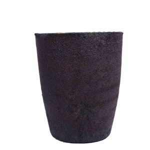
(Silicon Carbide Crucibles)
Silicon carbide (SiC) is a covalent ceramic compound composed of silicon and carbon atoms arranged in a tetrahedral latticework framework, mainly existing in over 250 polytypic types, with 6H, 4H, and 3C being the most technologically relevant.
Its strong directional bonding conveys remarkable solidity (Mohs ~ 9.5), high thermal conductivity (80– 120 W/(m · K )for pure solitary crystals), and impressive chemical inertness, making it among one of the most robust products for severe settings.
The large bandgap (2.9– 3.3 eV) guarantees outstanding electrical insulation at area temperature level and high resistance to radiation damage, while its low thermal development coefficient (~ 4.0 × 10 ⁻⁶/ K) contributes to premium thermal shock resistance.
These intrinsic buildings are protected even at temperature levels exceeding 1600 ° C, permitting SiC to preserve architectural honesty under prolonged direct exposure to thaw metals, slags, and reactive gases.
Unlike oxide ceramics such as alumina, SiC does not react readily with carbon or type low-melting eutectics in minimizing atmospheres, a vital benefit in metallurgical and semiconductor processing.
When made right into crucibles– vessels developed to include and warm products– SiC surpasses standard materials like quartz, graphite, and alumina in both lifespan and procedure integrity.
1.2 Microstructure and Mechanical Stability
The efficiency of SiC crucibles is closely connected to their microstructure, which depends on the manufacturing method and sintering additives used.
Refractory-grade crucibles are commonly produced using reaction bonding, where permeable carbon preforms are penetrated with liquified silicon, developing β-SiC with the reaction Si(l) + C(s) → SiC(s).
This process generates a composite framework of key SiC with recurring complimentary silicon (5– 10%), which improves thermal conductivity but might restrict use over 1414 ° C(the melting point of silicon).
Alternatively, completely sintered SiC crucibles are made through solid-state or liquid-phase sintering making use of boron and carbon or alumina-yttria additives, accomplishing near-theoretical density and higher purity.
These show superior creep resistance and oxidation stability yet are extra expensive and difficult to produce in large sizes.
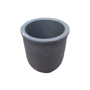
( Silicon Carbide Crucibles)
The fine-grained, interlocking microstructure of sintered SiC supplies superb resistance to thermal exhaustion and mechanical erosion, essential when handling molten silicon, germanium, or III-V compounds in crystal development procedures.
Grain border design, consisting of the control of second stages and porosity, plays an essential function in identifying long-lasting sturdiness under cyclic heating and aggressive chemical environments.
2. Thermal Performance and Environmental Resistance
2.1 Thermal Conductivity and Warmth Circulation
One of the defining benefits of SiC crucibles is their high thermal conductivity, which allows quick and consistent warm transfer throughout high-temperature handling.
In comparison to low-conductivity materials like fused silica (1– 2 W/(m · K)), SiC effectively distributes thermal energy throughout the crucible wall surface, lessening localized locations and thermal gradients.
This uniformity is vital in processes such as directional solidification of multicrystalline silicon for photovoltaics, where temperature level homogeneity straight impacts crystal top quality and flaw thickness.
The mix of high conductivity and low thermal growth leads to a remarkably high thermal shock parameter (R = k(1 − ν)α/ σ), making SiC crucibles immune to fracturing during rapid heating or cooling down cycles.
This enables faster furnace ramp rates, boosted throughput, and reduced downtime as a result of crucible failing.
In addition, the product’s capacity to hold up against repeated thermal biking without significant deterioration makes it excellent for batch handling in industrial furnaces running above 1500 ° C.
2.2 Oxidation and Chemical Compatibility
At elevated temperatures in air, SiC goes through easy oxidation, forming a safety layer of amorphous silica (SiO ₂) on its surface area: SiC + 3/2 O TWO → SiO TWO + CO.
This glazed layer densifies at high temperatures, functioning as a diffusion barrier that slows additional oxidation and preserves the underlying ceramic framework.
Nevertheless, in minimizing atmospheres or vacuum cleaner problems– common in semiconductor and steel refining– oxidation is subdued, and SiC continues to be chemically steady against liquified silicon, aluminum, and several slags.
It stands up to dissolution and response with liquified silicon approximately 1410 ° C, although long term direct exposure can lead to mild carbon pickup or interface roughening.
Most importantly, SiC does not introduce metallic contaminations into delicate melts, a crucial need for electronic-grade silicon manufacturing where contamination by Fe, Cu, or Cr has to be kept listed below ppb levels.
Nonetheless, care should be taken when processing alkaline planet steels or highly responsive oxides, as some can corrode SiC at extreme temperature levels.
3. Manufacturing Processes and Quality Assurance
3.1 Manufacture Methods and Dimensional Control
The manufacturing of SiC crucibles involves shaping, drying out, and high-temperature sintering or infiltration, with approaches selected based upon required purity, dimension, and application.
Common forming techniques include isostatic pressing, extrusion, and slip casting, each providing various degrees of dimensional precision and microstructural uniformity.
For huge crucibles used in solar ingot spreading, isostatic pushing guarantees constant wall density and thickness, decreasing the danger of asymmetric thermal expansion and failing.
Reaction-bonded SiC (RBSC) crucibles are economical and commonly made use of in factories and solar markets, though recurring silicon limitations maximum service temperature level.
Sintered SiC (SSiC) versions, while a lot more expensive, deal exceptional pureness, toughness, and resistance to chemical attack, making them ideal for high-value applications like GaAs or InP crystal development.
Accuracy machining after sintering may be required to achieve limited resistances, especially for crucibles utilized in vertical slope freeze (VGF) or Czochralski (CZ) systems.
Surface completing is critical to minimize nucleation sites for defects and make certain smooth melt circulation throughout spreading.
3.2 Quality Assurance and Efficiency Validation
Extensive quality control is important to guarantee reliability and longevity of SiC crucibles under demanding functional conditions.
Non-destructive assessment strategies such as ultrasonic screening and X-ray tomography are used to detect internal cracks, gaps, or density variations.
Chemical evaluation using XRF or ICP-MS validates low levels of metallic contaminations, while thermal conductivity and flexural toughness are gauged to verify material uniformity.
Crucibles are often based on substitute thermal biking examinations prior to delivery to recognize prospective failure modes.
Batch traceability and qualification are typical in semiconductor and aerospace supply chains, where component failing can result in pricey manufacturing losses.
4. Applications and Technical Effect
4.1 Semiconductor and Photovoltaic Industries
Silicon carbide crucibles play an essential duty in the production of high-purity silicon for both microelectronics and solar cells.
In directional solidification heating systems for multicrystalline solar ingots, large SiC crucibles work as the key container for molten silicon, withstanding temperatures over 1500 ° C for several cycles.
Their chemical inertness stops contamination, while their thermal stability guarantees consistent solidification fronts, leading to higher-quality wafers with less dislocations and grain borders.
Some manufacturers coat the inner surface area with silicon nitride or silica to further minimize adhesion and facilitate ingot launch after cooling down.
In research-scale Czochralski growth of compound semiconductors, smaller SiC crucibles are made use of to hold melts of GaAs, InSb, or CdTe, where marginal reactivity and dimensional security are extremely important.
4.2 Metallurgy, Shop, and Emerging Technologies
Past semiconductors, SiC crucibles are essential in steel refining, alloy prep work, and laboratory-scale melting procedures including light weight aluminum, copper, and rare-earth elements.
Their resistance to thermal shock and erosion makes them ideal for induction and resistance heating systems in shops, where they outlast graphite and alumina choices by numerous cycles.
In additive manufacturing of responsive steels, SiC containers are utilized in vacuum cleaner induction melting to stop crucible failure and contamination.
Emerging applications include molten salt reactors and focused solar power systems, where SiC vessels might consist of high-temperature salts or liquid metals for thermal power storage.
With recurring breakthroughs in sintering innovation and finishing design, SiC crucibles are poised to sustain next-generation materials processing, enabling cleaner, much more reliable, and scalable industrial thermal systems.
In recap, silicon carbide crucibles stand for a crucial allowing innovation in high-temperature product synthesis, integrating exceptional thermal, mechanical, and chemical performance in a single engineered element.
Their extensive adoption throughout semiconductor, solar, and metallurgical sectors highlights their duty as a keystone of contemporary commercial ceramics.
5. Distributor
Advanced Ceramics founded on October 17, 2012, is a high-tech enterprise committed to the research and development, production, processing, sales and technical services of ceramic relative materials and products. Our products includes but not limited to Boron Carbide Ceramic Products, Boron Nitride Ceramic Products, Silicon Carbide Ceramic Products, Silicon Nitride Ceramic Products, Zirconium Dioxide Ceramic Products, etc. If you are interested, please feel free to contact us.
Tags: Silicon Carbide Crucibles, Silicon Carbide Ceramic, Silicon Carbide Ceramic Crucibles
All articles and pictures are from the Internet. If there are any copyright issues, please contact us in time to delete.
Inquiry us