1. Product Fundamentals and Architectural Attributes of Alumina Ceramics
1.1 Crystallographic and Compositional Basis of α-Alumina
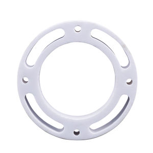
(Alumina Ceramic Substrates)
Alumina ceramic substrates, primarily made up of aluminum oxide (Al ₂ O TWO), function as the foundation of contemporary electronic product packaging due to their remarkable balance of electrical insulation, thermal stability, mechanical toughness, and manufacturability.
One of the most thermodynamically steady stage of alumina at high temperatures is diamond, or α-Al Two O TWO, which crystallizes in a hexagonal close-packed oxygen latticework with light weight aluminum ions occupying two-thirds of the octahedral interstitial websites.
This dense atomic plan conveys high firmness (Mohs 9), superb wear resistance, and strong chemical inertness, making α-alumina ideal for extreme operating atmospheres.
Commercial substrates typically contain 90– 99.8% Al Two O TWO, with small additions of silica (SiO TWO), magnesia (MgO), or unusual planet oxides made use of as sintering aids to advertise densification and control grain development during high-temperature processing.
Higher purity qualities (e.g., 99.5% and above) show remarkable electric resistivity and thermal conductivity, while reduced purity variants (90– 96%) offer cost-efficient options for less demanding applications.
1.2 Microstructure and Issue Engineering for Electronic Reliability
The efficiency of alumina substrates in electronic systems is seriously based on microstructural uniformity and issue minimization.
A penalty, equiaxed grain framework– usually ranging from 1 to 10 micrometers– makes sure mechanical honesty and decreases the possibility of split propagation under thermal or mechanical anxiety.
Porosity, particularly interconnected or surface-connected pores, need to be lessened as it deteriorates both mechanical strength and dielectric efficiency.
Advanced processing strategies such as tape spreading, isostatic pressing, and regulated sintering in air or managed atmospheres enable the production of substratums with near-theoretical thickness (> 99.5%) and surface area roughness listed below 0.5 µm, crucial for thin-film metallization and wire bonding.
Additionally, pollutant partition at grain borders can result in leakage currents or electrochemical migration under prejudice, requiring strict control over resources pureness and sintering problems to guarantee long-term reliability in moist or high-voltage settings.
2. Production Processes and Substratum Fabrication Technologies
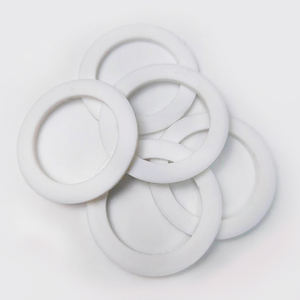
( Alumina Ceramic Substrates)
2.1 Tape Casting and Environment-friendly Body Processing
The manufacturing of alumina ceramic substratums starts with the preparation of an extremely spread slurry containing submicron Al ₂ O two powder, organic binders, plasticizers, dispersants, and solvents.
This slurry is processed using tape spreading– a continual technique where the suspension is spread over a relocating provider movie utilizing a precision doctor blade to accomplish uniform density, commonly between 0.1 mm and 1.0 mm.
After solvent evaporation, the resulting “green tape” is adaptable and can be punched, pierced, or laser-cut to develop via openings for upright interconnections.
Multiple layers may be laminated flooring to produce multilayer substratums for complex circuit integration, although most of industrial applications use single-layer setups because of cost and thermal expansion considerations.
The environment-friendly tapes are then carefully debound to get rid of natural ingredients with regulated thermal disintegration before last sintering.
2.2 Sintering and Metallization for Circuit Assimilation
Sintering is conducted in air at temperatures in between 1550 ° C and 1650 ° C, where solid-state diffusion drives pore removal and grain coarsening to accomplish complete densification.
The straight shrinking throughout sintering– typically 15– 20%– must be precisely forecasted and made up for in the layout of eco-friendly tapes to make certain dimensional precision of the final substratum.
Following sintering, metallization is applied to form conductive traces, pads, and vias.
2 primary methods dominate: thick-film printing and thin-film deposition.
In thick-film modern technology, pastes including metal powders (e.g., tungsten, molybdenum, or silver-palladium alloys) are screen-printed onto the substrate and co-fired in a decreasing environment to develop durable, high-adhesion conductors.
For high-density or high-frequency applications, thin-film processes such as sputtering or dissipation are used to down payment attachment layers (e.g., titanium or chromium) adhered to by copper or gold, allowing sub-micron pattern by means of photolithography.
Vias are loaded with conductive pastes and fired to establish electric interconnections between layers in multilayer layouts.
3. Useful Features and Efficiency Metrics in Electronic Equipment
3.1 Thermal and Electrical Behavior Under Functional Tension
Alumina substrates are valued for their beneficial mix of modest thermal conductivity (20– 35 W/m · K for 96– 99.8% Al ₂ O SIX), which makes it possible for efficient heat dissipation from power devices, and high volume resistivity (> 10 ¹⁴ Ω · centimeters), making certain very little leakage current.
Their dielectric continuous (εᵣ ≈ 9– 10 at 1 MHz) is stable over a broad temperature and frequency variety, making them ideal for high-frequency circuits as much as several ghzs, although lower-κ products like light weight aluminum nitride are liked for mm-wave applications.
The coefficient of thermal development (CTE) of alumina (~ 6.8– 7.2 ppm/K) is sensibly well-matched to that of silicon (~ 3 ppm/K) and certain product packaging alloys, decreasing thermo-mechanical anxiety during tool procedure and thermal biking.
Nevertheless, the CTE inequality with silicon stays an issue in flip-chip and direct die-attach setups, commonly requiring compliant interposers or underfill products to alleviate fatigue failure.
3.2 Mechanical Effectiveness and Environmental Durability
Mechanically, alumina substrates show high flexural toughness (300– 400 MPa) and excellent dimensional stability under load, enabling their usage in ruggedized electronics for aerospace, automobile, and industrial control systems.
They are resistant to vibration, shock, and creep at raised temperatures, keeping architectural integrity approximately 1500 ° C in inert atmospheres.
In humid settings, high-purity alumina reveals minimal moisture absorption and outstanding resistance to ion movement, making sure long-lasting reliability in outside and high-humidity applications.
Surface solidity likewise secures against mechanical damages throughout handling and assembly, although treatment needs to be taken to prevent side breaking because of integral brittleness.
4. Industrial Applications and Technological Impact Across Sectors
4.1 Power Electronic Devices, RF Modules, and Automotive Equipments
Alumina ceramic substratums are ubiquitous in power digital components, consisting of shielded gateway bipolar transistors (IGBTs), MOSFETs, and rectifiers, where they supply electrical isolation while helping with warmth transfer to warmth sinks.
In superhigh frequency (RF) and microwave circuits, they work as provider platforms for crossbreed integrated circuits (HICs), surface area acoustic wave (SAW) filters, and antenna feed networks because of their stable dielectric properties and low loss tangent.
In the automobile industry, alumina substratums are utilized in engine control devices (ECUs), sensing unit bundles, and electrical lorry (EV) power converters, where they endure heats, thermal biking, and direct exposure to corrosive liquids.
Their integrity under severe problems makes them crucial for safety-critical systems such as anti-lock stopping (ABDOMINAL MUSCLE) and progressed vehicle driver assistance systems (ADAS).
4.2 Medical Tools, Aerospace, and Arising Micro-Electro-Mechanical Solutions
Beyond customer and industrial electronic devices, alumina substrates are used in implantable medical gadgets such as pacemakers and neurostimulators, where hermetic sealing and biocompatibility are vital.
In aerospace and protection, they are used in avionics, radar systems, and satellite communication modules because of their radiation resistance and stability in vacuum cleaner atmospheres.
Furthermore, alumina is significantly used as an architectural and shielding system in micro-electro-mechanical systems (MEMS), consisting of pressure sensing units, accelerometers, and microfluidic gadgets, where its chemical inertness and compatibility with thin-film handling are beneficial.
As digital systems remain to require greater power thickness, miniaturization, and integrity under extreme conditions, alumina ceramic substratums continue to be a cornerstone product, linking the void between efficiency, expense, and manufacturability in advanced digital packaging.
5. Supplier
Alumina Technology Co., Ltd focus on the research and development, production and sales of aluminum oxide powder, aluminum oxide products, aluminum oxide crucible, etc., serving the electronics, ceramics, chemical and other industries. Since its establishment in 2005, the company has been committed to providing customers with the best products and services. If you are looking for high quality alumina silica, please feel free to contact us. (nanotrun@yahoo.com)
Tags: Alumina Ceramic Substrates, Alumina Ceramics, alumina
All articles and pictures are from the Internet. If there are any copyright issues, please contact us in time to delete.
Inquiry us